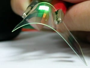
 Unlike traditional, synthetic LEDs (light-emitting diodes), OLED uses an organic substance that glows when an electric current is introduced. First OLED bear their origin to often quoted invention of Tang and Van Slyke in 1987, wherein a heterostructure device, much like its inorganic counterpart, yielded measurable light emission at voltages less than 10 V. Prior to this invention, only a faint glow came out of an OLED device at voltages on the order of 100 V. In most organic materials, the hole mobility is at least 10-100 times greater than that of an electron. Thus, the bilayer OLED reported in 1987, moved the recombination zone away from the cathode, leading to a better efficiency of the device. After more than 20 years of steady progress, OLEDs achieved efficiencies of more than 60Lm/W (which is comparable to that of the fluorescent light bulb) and lifetimes exceeding 100,000hours of operation. Modern OLEDs cover all visible spectra and go beyond that into near IR and UV. Two major applications of OLEDs include solid state lighting, where OLED offer efficient flexible thin and chip alternative to existing light sources and display area. In 2010 first OLED TVs (LG) and first OLED mobile displays (Samsung) hit the consumer electronics market. OLED displays truly represent the next generation display experience. Thin, light weight, wide viewing angles, large color gamuts, fast refresh rates and high contrasts are some of the reasons that the display industry is looking towards making OLED the next generation of display technology after LCD. In addition to superior display characteristics, OLED materials are inherently flexible, creating the possibility of foldable, bendable or rollable displays that will change our concept of a display and integrate into our world more than ever. Currently, OLEDs are used in today’s hottest smart phones, but it has been difficult for the industry to make OLED TVs at large scales for a reasonable price. One key reason for this is the inherent difficulty in patterning the red green and blue sub-pixels that make up the display, because the materials themselves are deposited in vacuum and are very sensitive to chemicals that may be used in a lithographic process. Alternative methods of patterning have been used for phones, such as fine metal mask (FMM) technology where the OLED materials are deposited through a metal stencil mask onto the substrate. This technique is difficult to scale and has resolution limitations. Other techniques include not patterning the OLED layer and using color filters to define the sub-pixel colors. Color filters reduce the energy efficiency and lifetime of the devices, however.
Our group in collaboration with Orthogonal Inc. (Rochester, NY) is developing solutions that will allow the direct patterning of OLED pixels using photolithography. Orthogonal solvents have been shown to be compatible with a range of solution processed and vacuum deposited OLED materials.
